
The CHIP process and prototype multifunctional device demonstration
Figure 1a illustrates the CHIP processing steps towards achieving a demonstration prototype of a 3D-integrated flexible optrode, which is typically used for neuronal recording with optogenetic stimulation. Initially, the microelectrodes, temperature sensors, and shielded μLEDs were co-designed but separately fabricated on Kapton substrates laminated on polydimethylsiloxane (PDMS)-coated glass handling substrates as polymer chiplets (#1–3). This strategy can ensure a high yield of each function using post-fabrication characterization before the CHIP bonding process. For the μLED chiplet fabrication, we leveraged transparent colorless Kapton and adopted a monolithically selective micro-transfer printing technique with metallization after the printing (Supplementary Fig. 1). An additional thin-film shielding interlayer was deposited and patterned on the backside of the μLED chiplet to prevent functional crosstalk. After the complete fabrication, the microelectrode and temperature sensor chiplets were directly peeled off from the handling substrates and were aligned and bonded onto the μLED chiplet sequentially using an room-temperature-(RT)-curing biocompatible epoxy resin. Finally, a UV-laser profiling completed the fabrication, achieving the CHIP process with a monolithic device ready to be peeled off from the handling substrate. Compared to the Si-based sequential fabrication process for double-sided functional integration23, this CHIP processing step is easy for double-sided area utilization by simply flipping device layers and bond them, and robust for 3D heterogeneous integration without extra physical, chemical, and thermal treatments for functional assembly7,26,27,30,31. Besides, if there is a need to achieve same-sided optical emitting and electrophysiological recording while still having the shielding function, there are potential strategies based on the CHIP process as follows: (i) turn the LED layer over and deposit exposed shielding windows just right on the top of the LED or the bottom of the electrode layer before the layer bonding; (ii) employ a flip-chip-bonding like method to print the μLEDs, thus the LED emitting surface naturally will be toward the same side as the recording electrodes.
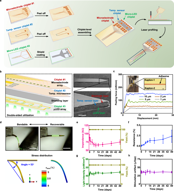
a Schematic illustration of the chiplet-level integration and device profiling approach, exemplified via manufacturing a 3D-integrated flexible optrode. b Left: The heterogeneously integrated multifunctionality includes electrophysiological recording (twelve microelectrodes, 10 × 20 μm2), temperature sensing (serpentine-shaped μ-resistor overlaying one μLED), optoelectronic shielding, and optical stimulating (6 μLEDs, 34 × 58 × 7 μm3). Right: The SEM images of the 3D-integrated shank (scale bar: 50 μm). c T-peeling test of the peeling force between two Kapton substrates with different adhesive thicknesses. The inset shows the measurement setup and the image of a test sample (scale bar: 1 μm). d Bendability and recoverability of the 3D-integrated flexible optrode (scale bar: 800 μm) and the simulation of its stress distribution during bending. e Measured impedance and microelectrode yield in the 3D-integrated optrode during the soak test. f Normalized resistance change of the temperature microsensor (20 nm thickness) during the soak test. g Measured light power and μLED yield in the 3D-integrated optrode during the soak test (input current 0.6 mA). h The recorded high-pass filtered peak-to-peak magnitudes of the stimulation artifact when all μLEDs were on in the 3D-integrated optrode (input current 1 mA). All soak tests were conducted in PBS solution at 47 °C for 7 weeks. All soak test data are presented as mean ± standard deviation of the mean (s.d.m.) (n = 6).
We implemented the chiplet functions using contemporary, flexible electronic designs (Fig. 1b). The prototype 3D-integrated flexible optrode comprised a linear array of microelectrodes (twelve poly(3,4-ethylenedioxythiophene)-poly(styrenesulfonate) (PEDOT:PSS)-based electrodes, site area: 10 × 20 μm2), a temperature microsensor (Pt-based serpentine-resistor), and a linear array of green-emitting μLEDs (six InGaN-based μLED chips with a lateral structure, chip area: 34 × 58 μm2) with a metal shielding interlayer (Au, thickness 100 nm) for optoelectronic shielding. The 3D-integrated flexible optrode with these three chiplets bonded from the CHIP process exhibited solid and tight bonding interfaces, as examined by cross-sectional SEM (Fig. 1b). Figure 1c shows the peeling force as a function of different adhesive thicknesses of 1–10 μm. Adhesives of more than 5-μm thick cured at RT showed forces of a similar magnitude as polyimide self-adhesion cured at a high temperature32. As a result, we used a 5-μm thick adhesive for the prototype optrode. Detailed specifications and fabrication processes are provided in Methods and Supplementary Fig. 2. The prototype 3D-integrated flexible optrode was constructed with a specification of ~75 μm thickness, 240 μm width, 2 mm length, and 27.5° tip angle. With this scheme, the optrode has excellent bending properties, cycling multiple times without an electrical open circuit during the bending, as shown in Fig. 1d and Supplementary Movie 1. This feature greatly differs from fragile Si-based optrodes5,6,22. The stress distribution simulation confirms the optrode’s robust bending ability with a maximal angle of 53°, which still results in less than 5% strain, which is typically considered as the fracture strain of gold films33. To better analyze the strain distribution during bending, we further studied the strain in each device layer (Supplementary Fig. 3). The neutral plane located around the interface between the LED layer and temperature sensor layer experienced zero deformation during bending. The LED layer at the top experienced a large stretching yet within the safe range (strain < 5%) when bent 53°. Besides, we also included a mechanical failure analysis (Supplementary Fig. 4) in which an extreme one-time bending was applied to the device (~108°). It was revealed that the LED located close to the base failed first while the other LED close to the tip still survived. The result is consistent with the prediction from the Finite Element Analysis (FEA) in which a significantly large strain appeared around the locations of the failed LED. The locations where the LED survived still showed a safe range of strain (<5%). What’s more, we also investigated the electrode impedance before, during, and after the bending (Supplementary Fig. 5). With the shank displacement from 0.5 to 1 mm, there were no obvious changes from the twelve electrodes on the shank before, during, and after the bending. On the other hand, the current CHIP-based optrode also inherits an instant insertion capability without an assisted stiff probe guide on a brain phantom34, as shown in Supplementary Figs. 6, 7 and Movie 2.
Another important feature of the CHIP process is that during this process, the I/O connections of all functional chiplets were located next to each other facing the same side, forming one monolithic I/O pad area by design. With the monolithic I/O design, the 3D-integrated optrode can be conveniently and rapidly mounted onto a PCB connector to achieve terminal control (Supplementary Fig. 8). Compared to other approaches such as using anisotropic conductive film (ACF), this non-permanent assembly method demonstrates robust contact pressure, efficient space utilization, and a cost-saving strategy in a replaceable and labor-effective manner. In addition to miniaturization, this multifunctional integration system from the CHIP process also demonstrated high reliability of the electrical recording, temperature sensing, optical emitting, and shielding capabilities while soaked in PBS solution at 47 °C for seven weeks, as shown in Fig. 1e–h. We also investigated the electrical, optical, and mechanical functions after cycled bending (Supplementary Fig. 9). It showed no obvious difference in their impedance and light emitting from 0 to 1000 time-cycled bending. Meanwhile, the SEM images still displayed a solid structure for the tip, neck, and base of the shank sidewall after a 1000-time cycled bending test.
Compared to state-of-the-art, Si-based electronic-photonic integrated optrodes (Supplementary Table 1), all of which were achieved from sequential fabrication, the CHIP process enables unprecedented multifunction incorporation yet with much-reduced manufacturing complexity and risk from the inherent parallelism in the new process flow. Compared to previous polymer-based devices from micro-scale stacking, CHIP allows easier processing from the chiplet-level operations without the risk of contaminating exposed sensors by over-flow adhesive from micro-scale shank on both sides during the pressure and bonding, which often demands larger width or area of the optrode for reliable bonding7. Handling plasma-treated or magnetic thin-film substrate in liquid environments to avoid such a problem is an alternative25,29. However, CHIP easily avoids common challenges in processing multiple functional shank stacking as well as the potential delamination or magnetic resonance interference after implantation. With the final-step laser profiling, CHIP can achieve highly miniaturized devices that are only limited by the sub-20-μm laser spot size, which is also continuously improving. On the other hand, chiplet-level processing can enable the mass production of many devices in parallel on the same 3D-integrated device. Leveraging existing wafer-level μLED transfer-printing techniques35, this manufacturability from CHIP holds immense potential in further scaling up toward wafer-level heterogeneous integration of polymer-based circuits (WHIP) for consumer-grade and low-cost products.
Characterizations of individual functions of the multifunctional device from CHIP
To evaluate the functionalities of the 3D-integrated flexible optrode from CHIP, we investigated its electrical recording, optical emitting, and thermal sensing capabilities through systematic experiments and simulations. Figure 2a illustrates the histogram of the impedances from the microelectrodes. These PEDOT:PSS-based electrodes possess a uniform green color with around 70–85 kΩ impedance (1 kHz) and are suitable for recording bio-electric activities36,37, implying that the CHIP process at RT has a potential advantage for integrating heat-sensitive materials such as PEDOT:PSS which suffers a non-recoverable electrical property degradation from thermal processing38,39. More information about the properties of these uniform PEDOT:PSS-based electrodes can be found in a recent study40. The μLED of the optrode shows a standard 525-nm emission peak wavelength under the current injection (Fig. 2b), matching many opsins’ optical absorption41. We also created independently addressed systems for the optical array with many μLEDs (Supplementary Movie. 3), enabling arbitrary optical stimulation combinations across different depths in the future. The shielding coating further strengthened the output optical power (Fig. 2c), presumably due to increased optical reflection from the backside metal shielding layer42. At an injection current of 1 mA, the individual green μLED achieved an irradiance of ~70 mW/mm2, sufficiently meeting the activation threshold of 1 mW/mm² for optogenetic modulation43,44. This light emission is contributed by the transparent colorless Kapton substrate rather than the brown-colored one used for μLED heterogeneous integration. Besides, we also included the light emission within the agarose gel environment (0.6%) (Supplementary Fig. 10). There were no significant differences when light penetrated through the same thick glass and agarose gel. Both non-shielded and shielded optrodes can maintain nearly Lambertian emission distributions (Fig. 2d). To illustrate the optrodes’ optical resolution, we established an optical propagation model in the brain tissue. Theoretical calculations indicate that light intensities from the optrode decrease to 5–30% of the original values over a propagating distance of 50 to 150 μm (Supplementary Fig. 11). We also analyzed the excitation spatial coverage of the optrode for different currents (Supplementary Fig. 12) in which the effective simulation volume was estimated based on an intensity threshold value of 1 mW/mm2 45,46,47. The simulated optical propagation, following a Lambertian profile, validates the theoretical calculations (Fig. 2e). On the other hand, we also predicted the light propagation when there was a gap between the μLED and targeted neurons (Supplementary Fig. 13).
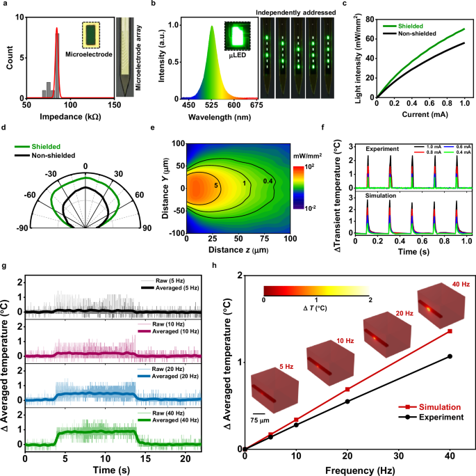
a The histogram of the electrode impedances in the microelectrode array in the integrated optrode. Inset and Right: the images of the single electrode and the array, respectively. b The measured wavelength spectrum of the μLED in the integrated optrode and the demonstrations of the independently addressable μLED array. c The measured surface light intensity of the μLED as a function of input current from both the non-shielded and shielded optrodes. d The measured light distribution of the μLED from both the non-shielded and shielded optrodes. e Simulated optical propagation of the μLED (40 mW/mm2 as an initial value). f Measured and simulated transient temperature rise as a function of input current (pulse duration 10 ms, frequency 5 Hz). g Temperature rises as a function of the frequency (pulse duration 10 ms, current 0.6 mA, total time 10 s). h Measured and simulated averaged temperature rise as a function of frequency (pulse duration 10 ms, current 0.6 mA). The simulated thermal effects correspond to the temperature distribution around the μLED with different stimulation frequencies. All the data of the measured temperature rise was obtained using an integrated temperature microsensor. All the optical and thermal simulation data were computed based on the brain tissue environment.
To mitigate potential bio-safety issues and unwanted biological responses caused by overheating, a temperature microsensor (Pt serpentine resistor, averaged sensitivity 0.00171/°C, Supplementary Fig. 14) was incorporated, overlaying the μLED close to the optrode base, with potentially the strongest heating effect. This location was chosen based on the smaller thermal capacitance in the shallower tissue environment. Figure 2f presents the measured and simulated transient temperature rises with different μLED injection currents. The results of the simulation are similar to the experimental findings. These results showed similar rises from 1 to 3 °C within a few milliseconds as the input current increases from 0.4 to 1 mA. The response time was faster than 4 ms, limited by the 250 Hz sampling rate (Supplementary Fig. 15). This rapid response suggests the feasibility of monitoring μLED temperature dynamics using the integrated temperature sensor. Investigations into the average temperature rise with varying stimulation frequencies (Fig. 2g, h) and duration times (Supplementary Fig. 16) indicated that the maximal average temperature rise remains below 1.5 °C, even with a maximal pulsed current injection of 0.6 mA (offering ~50 mW/mm2 light power) under conditions of 40 Hz frequency and 50 ms duration time. Normally, temperature increases of a few degrees in vivo are considered acceptable7,8,48. On the other hand, the optical intensity range of 1–10 mW/mm2 is considered sufficient for optogenetic modulation49,50,51. The steady-state heat transfer simulations including 6 μLEDs configured as the real device were established to investigate the thermal effect in the extreme scenario in which all of them are turned on simultaneously (Supplementary Fig. 17). It was revealed that the multiple temperature rise peaks were aligned with the location of each μLEDs. The maximum discrepancy in temperature peak between μLEDs (center to edge) is around 0.3 °C (frequency 40 Hz, duration 20 ms, current 0.6 mA). It should be emphasized that this is also an extreme stimulation condition. For a general 10 Hz, 10-ms duration protocol, the maximum temperature discrepancy between μLEDs is around 0.04 °C.
Thus, the 3D-integrated flexible optrode from CHIP offers high-density, individually addressable optical stimulation capabilities with sufficient light power and the ability to monitor the temperature rise in real-time for bio-safety. While the material choice, optrode design, and device footprint are all with in vivo applications in mind, future studies should conduct rigorous biocompatibility evaluations according to ISO 10993–1 for translation of this technology.
Optoelectronic artifacts in polymer-based electronic-photonic integrated devices
Effectively minimizing optoelectronic artifacts to ensure high-fidelity bio-signal acquisition poses a challenge for all bio-integrated electronic-photonic systems. Different from previous Si-based integrated optrodes, polymer-based devices consisting of ultra-thin transparent polymeric encapsulation/substrate layers are exempted from the substrate photovoltaic effect6,52. However, the densely distributed metal interconnections of the active and passive device components from different layers inherently introduce the possibility of electrical-induced artifacts, such as inductive-induced artifacts associated with electromagnetic interference (EMI)6,53 and capacitive-induced artifacts associated with electrostatic effects54. In addition, light can also lead to photoelectrochemical effects45,55 when active photons radiate to the electrode surface or hetero-junction interface from scattering. To mitigate the above stimulation artifacts, an effective strategy involves optoelectronic shielding between the μLED and electrode layers6,25,28,56. Such a shielding design was easily implemented using CHIP process. Here, we investigated the overall stimulation artifact of the 3D-integrated flexible optrode from CHIP with and without the shielding layer in Fig. 3.
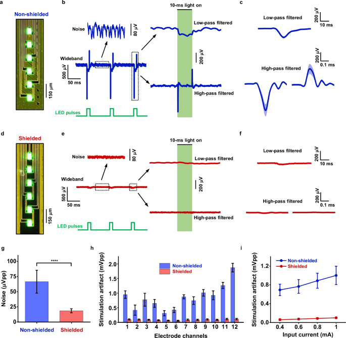
a Image of the non-shielded optrode with illumination of all μLEDs from the back side. b The waveforms of the recorded artifact on non-shielded optrode in the wideband and from low-pass and high-pass filtering. The data was analyzed from one representative electrode channel. c Averages of the low-pass and high-pass filtered waveforms based on the non-shielded optrode. d Image of the shielded optrode with illumination of all μLEDs from the back side. e The waveforms of the recorded artifact on shielded optrode in the wideband and from low-pass and high-pass filtering. The data is recorded from the same electrode location used in (b). f Averages of the low-pass and high-pass filtered waveforms from the channel based on the shielded optrode. g Statistical results of the recorded raw peak-to-peak magnitude of the noise for both the non-shielded and shielded optrodes. ****P < 0.0001. h Statistics of the recorded raw peak-to-peak magnitude of the stimulation artifact from twelve channels for both the non-shielded and shielded optrodes. All the μLEDs are turned on (pulse duration 10 ms, frequency 10 Hz, input current 1 mA for each μLED). i Statistics of the recorded raw peak-to-peak magnitude of the stimulation artifact from twelve channels with different input currents for both the non-shielded and shielded optrodes, where all the μLEDs are turned on (pulse duration 10 ms, frequency 10 Hz). All data are presented as mean ± standard deviation of the mean (s.d.m.) (n = 5).
Figure 3a displays the backside of the non-shielded optrode with illumination of all μLEDs, revealing densely packed parallel wires of the top μLEDs and bottom microelectrodes. Figure 3b illustrates recorded wideband, low-pass filtered, and high-pass filtered waveforms with the non-shielded optrode during pulsed illumination. The non-shielded optrode recorded a slow and mild peak within a low-frequency band and two fast and sharp opposite peaks corresponding to light-on and -off times within a high-frequency band. During the process, the non-shielded optrode also recorded a baseline noise of a large magnitude (~80 µVpp). Statistical results indicated a low-pass filtered averaged peak value of ~94 µV and a high-pass filtered peak-to-peak averaged value of ~519 µVpp (Fig. 3c). In Fig. 3d, the backside of the shielded optrode is depicted, where the metal shielded interlayer fully shields the recording microelectrode interconnection. With the shielding layer, a significantly reduced stimulation artifact was achieved under the same pulsed illumination parameters, as shown in Fig. 3e. The shielded optrode also exhibited significantly decreased baseline noise (~20 µVpp). Statistical results from the shielded optrode showed a low-pass filtered averaged peak value of ~22 µV, ~4 times smaller than the non-shielded one, and a high-pass filtered peak-to-peak averaged value of ~46 µVpp, ~11 times smaller than the non-shielded one (Fig. 3f). The magnitude of the baseline noise was also reduced by a factor of about 3.6 on average when operating with the shielded optrode, as illustrated in Fig. 3g. Analysis of stimulation artifacts from twelve electrode channels corresponding to all illuminated μLEDs underscore the shielding layer’s crucial role in suppressing artifacts across all electrode channels (Fig. 3h), and across all tested μLED drive current from 1 to 0.4 mA (Fig. 3i). Besides, we also compared the influences of the working environment on the electrical recording ability using shielded optrodes in PBS-based agarose gel (0.6%) (Supplementary Fig. 18). These were not greatly different in electrode impedance (average ~80 kΩ), noise (average ~20 μVpp), and stimulation artifacts (average ~40 μVpp) within the low- and high-frequency bands for the PBS or PBS-based agarose gel. It implies that the device by design has robust commonality in similar brain tissue environments. Therefore, the inter-layer shielding among these different functional chiplets from CHIP process establishes a low-noise, artifact-free flexible bio-integrated electronic-photonic design, and implementation.
Studies on the origin of the optoelectronic artifacts
To better understand the origins of optoelectronic artifacts in polymer-based devices as well as propose useful guidance for the design of all future flexible bio-integrated electronic-photonic systems, we conducted individually addressed μLED control for a detailed analysis of frequency-dependent artifacts, as illustrated in Fig. 4. In the non-shielded optrode, we observed a strong correlation between the locations of μLED and electrode site regarding the magnitude of artifact within a low-frequency band (Fig. 4a, b). Sequential illumination of an independent μLED site from #1 to #6 showed consistent changes in the magnitude of artifact recorded by neighboring electrode sites from #1 to #12 (Supplementary Fig. 19). These results imply that the artifact within the low-frequency band (1–300 Hz) is most likely attributed to the optical-related effect since each μLED primarily illuminates its neighboring electrode sites (Supplementary Fig. 20). The recorded waveforms are also consistent with the result of the light-induced artifacts from previous reports57,58. This postulation was further confirmed by the observation that when the LED common p-interconnect wire was disconnected, the optical-related waveform disappeared (Fig. 4b, right side). On the other hand, with the same sequential illumination of the independent μLED from #1 to #6, the artifacts within a high-frequency band (300–6000 Hz) depicted a complicated magnitude mapping, as shown in Fig. 4c. This magnitude distribution within the high-frequency band suggests an electrical-induced coupling underlying the artifacts instead of optical. To uncover the origin of this interference, we disconnected the μLED common p-interconnect wire and maintained the connection of the LED n-interconnect wires. Notably, even with no current flowing through each μLED, the electrode channels still could record sharp and fast waveforms of the same amplitude as the connected case within the high-frequency band (Fig. 4c, right side). We found that the recorded waveform only showed a single negative peak that responded to the voltage-on time. This phenomenon suggests that the artifact within the high-frequency band was mainly from the capacitive-induced coupling associated with the electrostatic effect (Supplementary Fig. 21) but not EMI. This finding is consistent with previous understanding that EMI-induced artifacts are much slower28,53, while capacitive coupling is much faster59. Besides, the recorded signal with the same amplitude, depending on input voltage regardless of whether there is current flowing through, suggests that the signal is being induced by an electric field rather than a magnetic field, which is characteristic of capacitive coupling60. The schematic illustration and simulation of the cross-section shank with different layered μLED and electrode wires in Fig. 4d further agreed well with the magnitude mapping of the artifacts in Fig. 4c. As depicted in Fig. 4d, the electrical field resulted from the fast-charging signals carrying on the bottom LED wires had propagated through the polymeric layers towards the top nearby electrode wires due to the electrostatic effects.
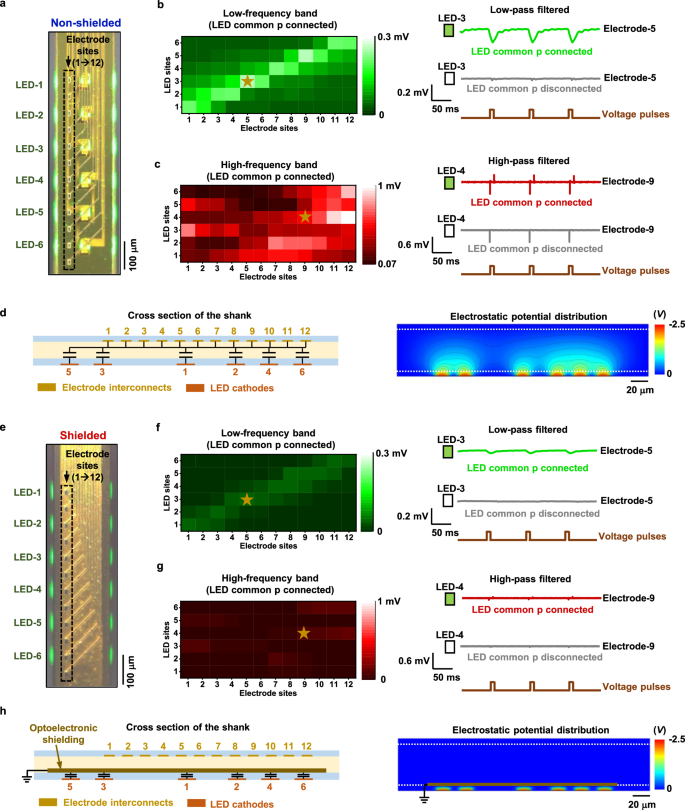
a The illustration of the μLED and electrode sites for the non-shielded optrode. The heat maps of the average recorded magnitude of stimulation artifact within the low-frequency band in (b) and within the high-frequency band in (c), with active single μLED from site 1 to site 6, based on the non-shielded optrode. The right side is the waveform comparison from the same channel (the graphic mark “star” from the left-side heat map) with and without μLED common p-connection from the low- and high-frequency bands, respectively. d Schematic illustration of the location of the μLED and electrode lines on the cross-section of the non-shielded polymer shank (twelve gold blocks: electrode recording interconnects, six orange blocks: μLED n-type driving interconnects, six equivalent plate capacitors between the μLED and electrode lines). The right side is a simulation of the electrostatic potential distribution from these μLED driving lines. e The illustration of the μLED and electrode sites for the shielded optrode. The heat maps of the average recorded magnitude of stimulation artifact within the low-frequency band in (f) and from the high-frequency band in (g), with active single μLED from site 1 to site 6, based on the shielded optrode. The right side is the waveform comparison from the same channel (the graphic mark “star” from the left-side heat map) with and without μLED common p-connection from the low- and high-frequency bands, respectively. h Schematic illustration of the location of the μLED and electrode interconnect on the cross-section of the shielded polymer shank (twelve gold blocks: electrode recording interconnects, six orange blocks: μLED n-type driving interconnects, a dark yellow block: optoelectronic shielding layer, six equivalent plate capacitors between the μLED driving lines and shielding layer). The right side is a simulation of the electrostatic potential distribution from these μLED driving lines when there is a shielding layer.
These hypotheses were further vindicated by the shielded optrode, where the microelectrodes were fully blocked from the μLED array’s direct optical radiation (Fig. 4e). We observed effectively suppressed artifacts in both the low- and high-frequency bands but with highly similar spatial patterns to the non-shielded case, where there is still the linear relationship for the low-frequency case while the similar enhanced magnitude patterns among others for the high frequency (Fig. 4f, g). We attribute the remaining low-frequency band artifacts to light scattering around the environment (Supplementary Fig. 22). For high-frequency band artifacts, we observed a similar single negative peak of the same magnitude when the μLED common p interconnect was disconnected, consistent with an electrostatic origin. The remaining electrostatic effect might be through the conductive medium surrounding the devices since the grounded shielding significantly mitigated the impact of the intra-device interference by more than two orders of magnitude from simulation (Fig. 4h and Supplementary Fig. 23).
link





More Stories
Researchers Reveal Molecular Secrets of Flexible Electronics
Growth Outweighs Uncertainty for Flexible and Printed Electronics: OE-A Survey
SEMI FlexTech Announces 2026 FLEXI Award Winners