


Bending tests of TCO/polymer sheets
Here, commercially available ITO/PEN sheets, which are commonly used in flexible electronic devices, were subjected to bending tests. Figure 1b is a top-view optical micrograph of the ITO/PEN sheet in the bent state (r = 7 mm), where the externally applied uniaxial tensile strain (εA) at the convex surface and near-surface region is 0.0089, as calculated using the equation εA = tS/2r (tS is the substrate thickness; ~125 μm for PEN)13,17. (Supplementary Fig. 1 plots the calculated applied uniaxial tensile universal strain (εA), as a function of r, and the corresponding stress (σA) within the layers studied here. For analysis of multiple layers, see Supplementary Note 113. Any tensile or compressive internal residual stresses within the individual layers would augment or diminish, respectively, the overall stresses in the layers in the bent state. Supplementary Table 1 lists the thicknesses of the different layers used in this study and their relevant static mechanical properties15,18,19,20,21,22,23,24,25,26). Under this applied stress, typical array of ‘channel’ cracks running parallel to the bending axis within the brittle ITO film are observed in Fig. 1b. Such observations have been reported in the flexible electronics literature on numerous occasions (see e.g. ref. 16). However, there have been no reports of substrate cracking in TCO/polymer sheets in the literature. This may be because, as mentioned earlier, it is generally assumed that the polymer substrate does not crack due to its extremely high toughness and substantial thickness relative to the TCO thin film (e.g. ITO thickness is ~300 nm, compared to PEN substrate thickness of ~125 μm)16. This purported assumption is supported by the observations in Fig. 1b where the ‘channel’ cracks in the ITO film do not appear to extend into the bare PEN substrate part without the ITO film (bottom region of Fig. 1b). However, this assumption is challenged by the scanning electron microscopy (SEM) observations of cross-sections created by focused ion beam (FIB) in Fig. 1c, d in the bent state (strained), which show cracking in the PEN substrate under the ITO film. It appears that the ‘channel’ cracks penetrate deep into the PEN substrate underneath. The cross-section SEM images in Fig. 1c,e confirm that the bare PEN substrate is uncracked. To further investigate the depth of the cracks in the PEN substrate, a longer ‘trench’ along the crack was FIB-cut, revealing deep cracks > 25 μm (Fig. 1f), which is ~20% of the total substrate thickness. To confirm that the substrate cracking was not due to the FIB-cutting process itself, part of the ITO in a previously bent (r = 7 mm) ITO/PEN sheet was removed by etching. Supplementary Fig. 2a, b present top-view SEM images of that specimen in the bent state, which clearly shows substrate cracking under the etched-away ITO. This type of extensive substrate cracking is observed consistently in many ‘channel’ cracks within the same ITO/PEN specimen, and also in different ITO/PEN specimens. Similar substrate-cracking behavior is observed in ITO(~300 nm)/PET(~125 μm) (Fig. 2a) and ITO( ~ 200 nm)/PI(~80 μm) (Fig. 2b) sheets, which are also commonly used in flexible electronic devices. Furthermore, substrate cracking is observed in multilayer devices built upon ITO/PEN sheets, e.g. flexible PSCs (Fig. 3), a promising new low-cost, lightweight PV technology6,27,28. It is important to note that no evidence for interfacial delamination was observed in Figs. 1d, 2a, b, and 3c. The key to the above substrate-cracking observations in the cross-sections, which have eluded past studies, is that we performed FIB-cutting and SEM imaging in situ in the bent state.

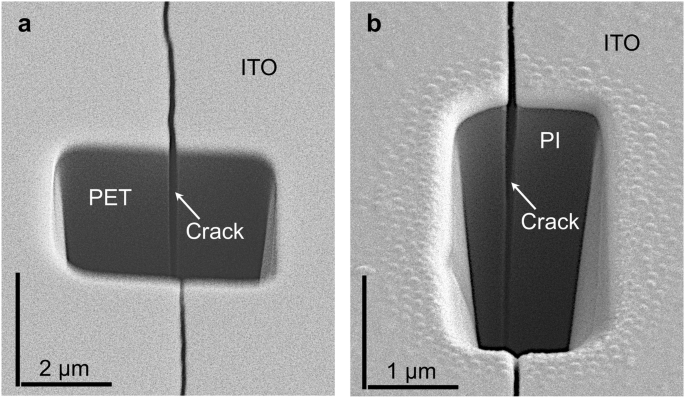
a, b SEM images of FIB-cut cross-sections of ‘channel’ cracks in bent ITO/PET to r = 7 mm (εA = 0.0089) (a) and ITO/PI to r = 5 mm (εA = 0.0080) (b) in the bent state (strained), showing cracking of both ITO films and substrates. (FIB-cutting was performed while in the bent state. All FIB-cut specimens were observed at a 52° forward tilt angle, hence vertical micron bar (representing depth) is longer than the horizontal one, as indicated.

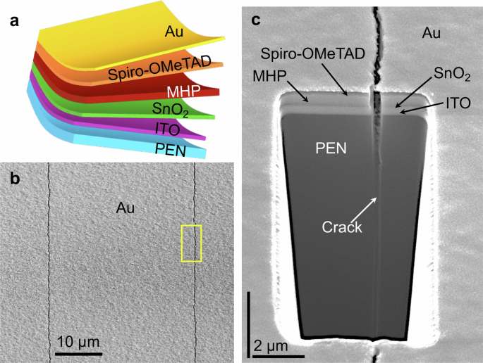
a Schematic illustration (not to scale) of the different layers in the flexible PSCs (exploded view). Here SnO2 and Spiro-OMeTAD serve as the electron-transport and hole-transport, respectively, layers. Metal halide perovskite (MHP) serves as the light absorber material, and Au is the top electrode. b, c SEM images of a working (19.7% efficiency) flexible PSC bent to r = 7 mm, in the bent state (strained), showing top-surface view of ‘channel’ cracks (b), and FIB-cut cross-section from an area indicated by the yellow rectangle in (b) of a ‘channel’ crack revealing cracking in all the layers in the flexible PSC and the PEN substrate (c). (FIB-cutting was performed while in the bent state from a region similar to that indicated by the yellow rectangle in (b). All FIB-cut specimens were observed at a 52° forward tilt angle, hence vertical micron bar (representing depth) is longer than the horizontal one, as indicated in (c).
This demonstration of substrate cracking in TCO/polymer sheets is significant because it raises serious questions about the prevailing notion that high-toughness polymer substrates are immune to cracking. The current design, manufacturing, and operation of flexible electronic devices are based on this notion. Since the substrate serves as the foundational ‘bedrock’ of any flexible device, substrate cracking seriously undermines the mechanical integrity and reliability of the entire device, making it susceptible to cyclic fatigue and other time-dependent failure mechanisms, such as creep and environment-assisted cracking or degradation.
Mechanics of substrate cracking
There have been a few studies reporting cracking in compliant, tough polymer substrates, such as PDMS, PET, and PI underneath either stiff, ductile metal films (Au/PDMS29, Al/PDMS30) or stiff, brittle ceramic films (SiNx/PET, SiNx/PI31). (Note that while Kim et al.31 show visual evidence for substrate cracking in cross-sections of SiNx/PET, those cracks formed only after holding the specimens in tension for 5 days under ambient conditions). Cracking has also been reported in compliant, tough brass substrates underneath stiff, brittle TiN films32. However, in all these cases the substrate cracking is modest, and to the best of our knowledge there have been no published reports of substrate cracking in TCO/polymer sheets and related flexible electronic devices.
To understand the genesis of the substrate-cracking phenomenon, we look back at some previous mechanics studies where cracking of compliant substrates underneath stiff films has been predicted and modeled33,34,35,36,37. For example, analytical modeling by Gecit34 indicates that when a putative crack of depth, c, in a stiff film of thickness, h, (Al or steel) under uniaxial tension approaches the interface with a compliant substrate (epoxy or Al), the crack-driving stress intensity factor, Kh, increases dramatically relative to reference Ko for no elastic mismatch between the film and the substrate. This is the result of concentrated shear stresses induced in the substrate at the crack-interface intersection due to the elastic mismatch35, and it is depicted schematically in Supplementary Fig. 3a. It is implied that the substrate is expected to crack, but experimental evidence for the same is not provided in those papers33,34,35,36,37. By corollary, when the elastic mismatch is reversed, i.e. compliant film (Al) on stiff substrate (steel), the Kh diminishes.
Here it is instructive to define the elastic mismatch between the film (F) and the substrate (S) in terms of the Dundur’s parameters, α and β, which incorporate not only their respective Young’s moduli (EF, ES) but also shear moduli (μF, μS) and Poisson’s ratios (νF, νS)38:
$${\rm{\alpha }}=\frac{\bar{{E}_{{\rm{F}}}}-\bar{{E}_{{\rm{S}}}}}{\bar{{E}_{{\rm{F}}}}+\bar{{E}_{{\rm{S}}}}}$$
(1)
$$\beta =\frac{1}{2}\frac{{{\rm{\mu }}}_{{\rm{F}}}\left(1-2{{\rm{\nu }}}_{{\rm{S}}}\right)-{{\rm{\mu }}}_{{\rm{S}}}(1-2{{\rm{\nu }}}_{{\rm{F}}})}{{{\rm{\mu }}}_{{\rm{F}}}\left(1-{{\rm{\nu }}}_{{\rm{S}}}\right)+{{\rm{\mu }}}_{{\rm{S}}}(1-{{\rm{\nu }}}_{{\rm{F}}})}$$
(2)
where Ē = E/(1-ν2) is the plane-strain Young’s modulus. Using the Gecit model34, we calculate the normalized stress intensity factor \({\hat{k}}_{n}\)=Kh/Ko for a putative mode I tensile crack of normalized length \(\hat{c}\)=c/h in ITO/PEN, ITO/PET, and ITO/PI film/substrate bilayer combinations specifically, whose Dundur’s parameters are listed in Supplementary Table 2 and plotted in Fig. 4b (see Supplementary Note 2 for modeling details34,39). An incipient crack (small \(\hat{c}\)) at the surface of the film loaded in uniaxial tension (as in the bending test) will propagate when Kh ≥ KIC condition is satisfied, where KIC is the fracture toughness of the film. In such a loading situation, Ko ∝ c0.5, and, thus, the crack is expected to propagate unstably40. The results in Fig. 4a show that, due to the presence of the compliant substrate, Kh for a crack in the film increases with \(\hat{c}\), beyond the conventional c0.5-scaling increase represented by \({\hat{k}}_{n}\) = 1. The \({\hat{k}}_{n}\) then rises dramatically as the crack approaches the interface (\(\hat{c}\) → 1), and induces a stress intensity factor in the substrate at the interface that approaches infinity. The singularity implies that, in principle, the crack will continue to propagate into the substrate regardless of the substrate toughness, as hypothesized by Gecit34 and Beuth35,36. Fig. 4d-e schematically depict this substrate-cracking behavior. By corollary, in the absence of the film, the substrate would otherwise not crack due to its very high fracture toughness (Fig. 4c). Once the crack enters the substrate (\(\hat{c}\) > 1), \({\hat{k}}_{n}\) is expected to decrease as the crack propagates deeper into the substrate, an effect modeled by Thouless, et al.37. In the case of bending, the applied σA experienced by the crack tip also decreases as it propagates deeper into the substrate, and the stress goes to zero at the neutral axis, before becoming compressive13. Thus, cracks in the substrate are limited to ~20% of its thickness, but are sufficiently deep to cause cracking-induced degradation of the device.

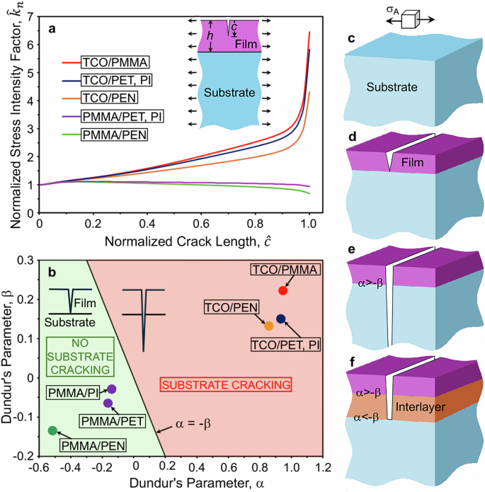
a Plot of \({\hat{k}}_{n}\) (= Kh/Ko) as function of \(\hat{c}\) (= c/h) for different film/substrate combinations relevant to this study. Inset: schematic illustration (not to scale) of the crack of depth, c, in the film of thickness, h. b Design map of the two Dundur’s parameters (α and β) for film/substrate showing the boundary (α = -β) between substrate-cracking (α > -β) and crack-arrest (α < -β) regions. The film/substrate combinations in (a) are indicated on the map in (b). c−f Schematic illustrations (not to scale) of cracking behavior under uniaxial tensile loading depicting no substrate cracking (c), ‘channel’ crack in film (d), extension of crack into the substrate (e), and substrate-cracking mitigation approach using an interlayer (f).
Substrate-cracking mitigation
Using the Gecit model34, we have constructed a design map in Fig. 4b, where for α > -β, \({\hat{k}}_{n}\) is expected to increase dramatically as the crack approaches the interface (\(\hat{c}\) → 1), resulting in substrate cracking. By corollary, \({\hat{k}}_{n}\) will decrease with \(\hat{c}\) → 1 for α < -β, resulting in crack arrest at the interface. (Note that this map can also be derived from Zak-Williams analyis33). As expected, ITO/PEN, ITO/PET, and ITO/PI combinations lie in the substrate-cracking region on the map in Fig. 4b. (IZO included in this map is another popular TCO that is used in this study, and its elastic properties are very similar to those of ITO (see Supplementary Table 1).) Since the much stiffer ITO (or IZO) film is key to the substrate-cracking problem, one can envision replacing the TCO with alternate, less stiff transparent-conducting electrodes made of polymers, metal meshes, or carbon-based nanomaterials41. However, those alternate electrodes are typically inferior to TCO in terms of the combination of high optical transparency and low sheet resistance they can offer41.
Using the design map in Fig. 4b, which provides general guidelines, we have designed a simple approach here for mitigating the substrate-cracking problem in generic TCO/polymer sheets for flexible electronic devices, without the need to eliminate the TCO. Our approach entails the use of a transparent, compliant interlayer between the TCO and polymer substrate, such that α < -β for the interlayer/substrate combination. To demonstrate the proof-of-concept, a polymethyl methacrylate (PMMA) interlayer (E ~ 3 GPa19) is chosen for insertion between IZO film (E ~ 130 GPa22) and PEN substrate (E ~ 9 GPa15) (Supplementary Table 1). Figure 4a plots \({\hat{k}}_{n}\) as a function of \(\hat{c}\) for the IZO/PMMA and PMMA/PEN combinations, whose Dundur’s parameters are listed in Supplementary Table 2 and plotted in Fig. 4b. For the IZO/PMMA case, a very rapid rise in \({\hat{k}}_{n}\) is observed as the crack approaches the interface, commensurate with the large α and β for that combination. Thus, a putative crack in IZO film is expected to propagate into the PMMA interlayer underneath, as depicted schematically in Fig. 4f. However, in the case of the PMMA/PEN combination, for the same putative crack in the PMMA layer, \({\hat{k}}_{n}\) diminishes as the crack approaches the PMMA/PEN interface. This is due to the reversal of the concentrated shear stresses induced in the substrate due to the elastic mismatch (Supplementary Fig. 3b). Therefore, the crack is expected to be arrested, precluding any substrate cracking (Fig. 4f). While the approach of introducing interlayers between dissimilar materials for mitigating cracking has been discussed before (see e.g42,43), this approach has eluded application to TCO/polymer sheets and related flexible electronic devices. To test this hypothesis experimentally, PMMA layers of different thicknesses ( ~ 250, ~300, ~400, and ~600 nm) were spin-coated onto PEN substrates. Unfortunately, PMMA is unable to withstand the processing conditions of the subsequent IZO deposition. Therefore, an ultrathin, transparent layer of amorphous SiO2 (~5 nm) was e-beam evaporated on the PMMA surface to protect it. Considering the thinness of the SiO2, it is not expected to interfere with this mitigation approach. IZO ( ~ 250 nm thickness) was then sputter-deposited on top of the SiO2. In the case of no-PMMA, substrate cracking is observed in the FIB-cut cross-section in Fig. 5a, which is similar to that in the ITO/PEN case (Fig. 1d). Similarly, in the case of 250-nm PMMA interlayer, cracking of the PEN substrate is observed in Fig. 5b. However, dramatic arrest of ‘channel’ cracks at the PMMA/PEN interface is observed in Fig. 5c with a ~ 300 nm PMMA interlayer. The existence of an interlayer critical thickness for effective substrate-crack mitigation is related to the length scale of the crack-tip stress field relative to the interlayer thickness. (This effect is not considered in the mechanics models discussed earlier.) Similar crack-arrest behavior is observed in Fig. 5d with a thicker PMMA interlayer ( ~ 600 nm). It is important to note that no evidence for interfacial delamination was observed in Fig. 5a-d. (In related experiments, instead of the SiO2 protective layer, Au layers ( ~10 nm) were deposited before and after PMMA deposition, which allowed better contrast delineation of the PMMA layer in the SEM; the same type of crack-arrest behavior is observed with a ~ 400 nm PMMA interlayer (Supplementary Fig. 4). This indicates that a relatively thin PMMA interlayer is sufficient for suppressing substrate cracking. Thus, the design map in Fig. 4b, in conjunction with static elastic properties of the materials under consideration, can be used as a general guide for choosing a suitable transparent material for interlayer between the TCO film and the substrate to prevent substrate cracking in those devices. Of course, the transparency requirement on the interlayer is relaxed for use in otherwise opaque flexible electronic devices. It is acknowledged that the incorporation of an additional layer (interlayer) between TCO/substrate can make the multilayer stack more susceptible to interfacial delamination, which is highly undesirable from a device-reliability standpoint. Thus, to avoid any interfacial delamination, it is important to ensure that the interfaces are sufficiently tough, as was done in this study.

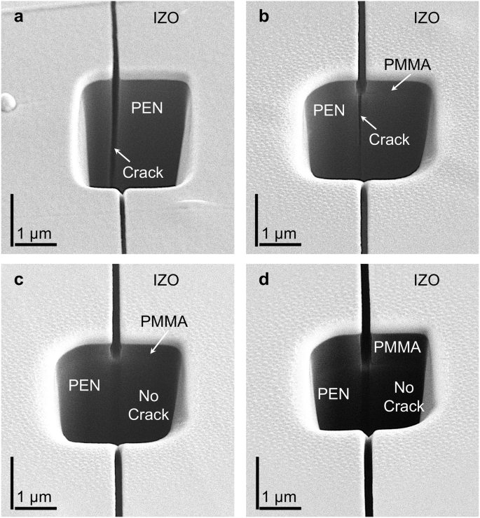
a−d SEM images of FIB-cut cross-sections of ‘channel’ cracks in combinations: IZO/PEN (a), IZO/PMMA(250 nm)/PEN (b), IZO/PMMA(300 nm)/PEN (c), and IZO/PMMA(600 nm)/PEN (d), bent to r = 7 mm (εA = 0.0089), in the bent state (strained). A thin SiO2 layer ( ~ 5 nm) was used on top of PMMA. (FIB cuts were made while in the bent state. All FIB-cut specimens observed at a 52° forward tilt angle, hence vertical micron bars (representing depth) are longer than the horizontal ones, as indicated in (a−d).
Electrical properties
The relative change in the resistance (ΔR/RO) of the ITO film on PEN substrate was measured at different bending radii, r, in the bent state (strained), where the resistance R is in the direction perpendicular to the bending axis (Supplementary Fig. 5a), RO is the initial resistance in the flat state (unstrained), and ΔR = R–RO. Beyond a critical bending radius (r = 10 mm), ITO’s ΔR/RO increases monotonically with decreasing r. Supplementary Fig. 5b plots the corresponding measured density of ‘channel’ cracks as a function of decreasing r, in the bent state, which also increases monotonically. It is assumed that the increase in the crack density in the ITO film is responsible for the increase in the relative change in the resistance in the bent state. However, when the ITO/PEN sheet is returned to the flat state (i.e. one bending cycle), ΔR/RO typically approaches zero. This is because the mating walls of ‘channel’ cracks in the ITO can make good contact in the flat state, although the cracks are not healed.
In light of the substrate-cracking behavior reported here, it is hypothesized that when the TCO/polymer sheet is subjected to cyclic bending (i.e. multiple cycles), the propensity for the substrate cracks to close properly when returned to the flat state will decrease progressively. This is likely due to the accumulation of debris within the substrate cracks, worsening misalignment of the mating crack walls, and the fatigue-induced propagation of the crack deeper into the substrate, with increasing number of cycles. This, in turn, is likely to progressively prevent the TCO crack walls from making good contact, thereby resulting in increasing ΔR/RO (flat state) with number of cycles, n. It is also hypothesized that in the case where substrate cracking is eliminated, e.g. in IZO/PMMA(300 nm)/PEN, the flat-state ΔR/RO may not increase with increasing n. These hypotheses are illustrated schematically in Supplementary Fig. 6. To verify these hypotheses, ΔR/RO of IZO/PEN sheets was measured in the flat state (Fig. 6) after subjecting them to bending cycles in the range n = 1 to 104, at bending radius r = 7 mm (εA = 0.0089) using a testing method described elsewhere28. Fig. 6 plots these data, which clearly show progressive increase in flat-state ΔR/RO with number of bending cycles, from ~0.1 to ~1,200 after 104 bending cycles. In contrast, no appreciable change in ΔR/RO could be measured in IZO/PMMA(~300 nm)/PEN in the flat state, even after 104 cycles where ΔR/RO ~ 0.5. These results reinforce the critical importance of substrate cracking in the degradation of TCO electrical properties. Since electrical continuity of the TCO film is key to the proper functioning of any multilayer device built upon TCO/polymer sheets, substrate cracking is highly detrimental for the durability and reliability of such devices.

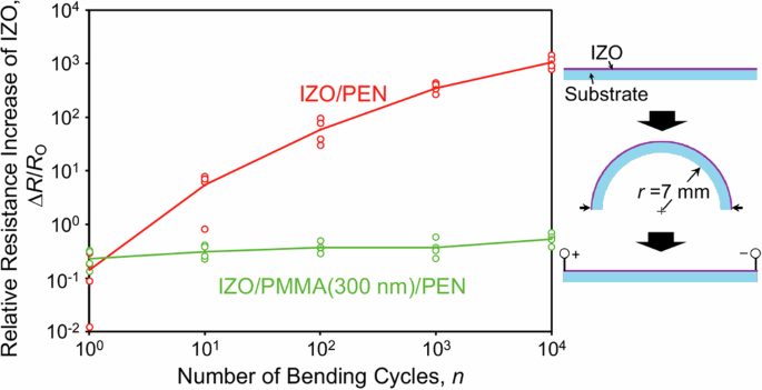
The relative increase in the DC electrical resistance of IZO film on PEN substrate, where the substrate cracks in bending (r = 7 mm; εA = 0.0089), in the flat state (unstrained) as a function of bending cycles, n. Corresponding measurements of IZO on PMMA(300 nm)/PEN substrate, where the substrate does not crack in bending. Measurements from four different specimens for each material system reported. The solid lines connect the averages. The schematic illustration (not to scale) on the right depicts one bending cycle: flat→bent→flat.
link