Electronic waste, or e-waste, is a rapidly growing global problem, and it is expected to worsen with the production of new kinds of flexible electronics for robotics, wearable devices, health monitors, and other new applications, including single-use devices.
Table of Contents
ToggleScalable manufacture of more complex multilayered circuits
A new kind of flexible substrate material developed at MIT, the University of Utah, and Meta has the potential to enable not only the recycling of materials and components at the end of a device’s useful life, but also the scalable manufacture of more complex multilayered circuits than existing substrates provide.
The development of this new material was described recently in the journal RSC: Applied Polymers, in a paper by MIT Professor Thomas J Wallin, University of Utah Professor Chen Wang, and seven others.
“We recognise that electronic waste is an ongoing global crisis that’s only going to get worse as we continue to build more devices for the internet of things, and as the rest of the world develops,” says Wallin, an assistant professor in MIT’s Department of Materials Science and Engineering.
To date, much academic research on this front has aimed at developing alternatives to conventional substrates for flexible electronics, which primarily use a polymer called Kapton, a trade name for polyimide.
Most such research has focused on entirely different polymer materials, but “that really ignores the commercial side of it, as to why people chose the materials they did to begin with”, says Wallin. Kapton has many advantages, including excellent thermal and insulating properties and ready availability of source materials.
The polyimide business is projected to be a $4bn global market by 2030. “It’s everywhere, in every electronic device basically,” including parts such as the flexible cables that interconnect different components inside your cellphone or laptop, says Wang.
It is also widely used in aerospace applications because of its high heat tolerance. “It’s a classic material, but it has not been updated for three or four decades,” he says.
However, it is also virtually impossible to melt or dissolve Kapton, so it cannot be reprocessed. The same properties also make it harder to manufacture the circuits into advanced architectures, such as multilayered electronics. The traditional way of making Kapton involves heating the material to anywhere from 200 to 300 degrees Celsius. “It’s a rather slow process. It takes hours,” says Wang.
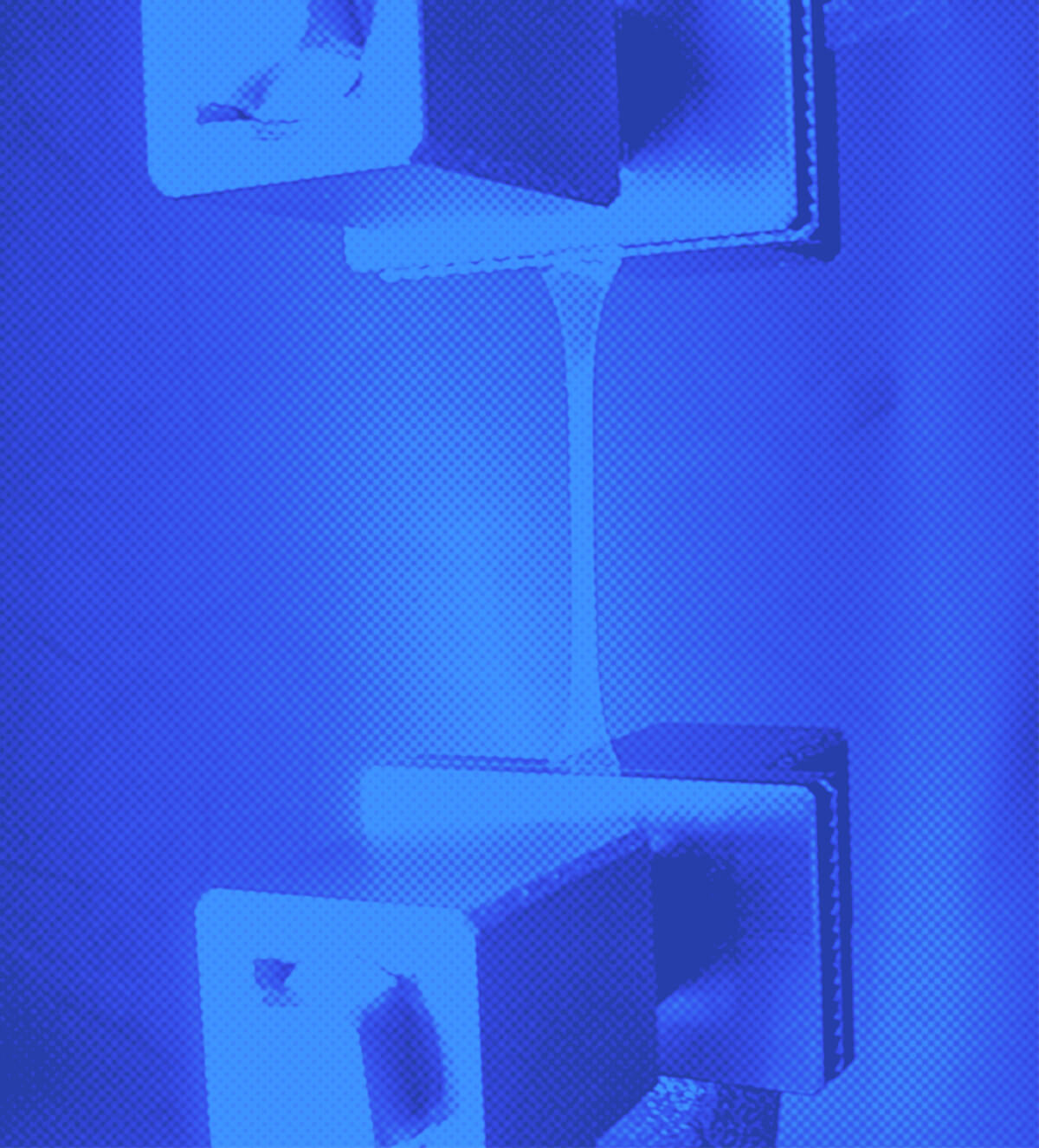
The alternative material that the team developed, which is itself a form of polyimide and therefore should be easily compatible with existing manufacturing infrastructure, is a light-cured polymer similar to those now used by dentists to create tough, durable fillings that cure in a few seconds with ultraviolet light. Not only is this method of hardening the material comparatively fast, it can operate at room temperature.
Processed at low-temperature
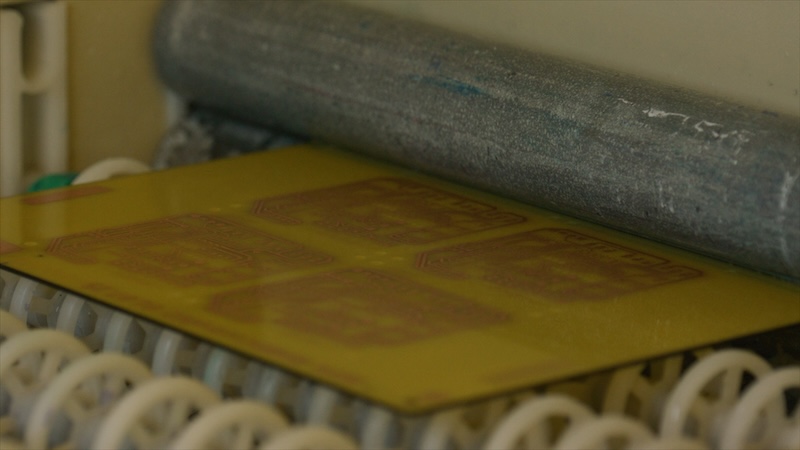
The new material could serve as the substrate for multilayered circuits, which provides a way of greatly increasing the number of components that can be packed into a small form factor.
Previously, since the Kapton substrate doesn’t melt easily, the layers had to be glued together, which adds steps and costs to the process. The fact that the new material can be processed at low-temperature while also hardening very quickly on demand could open up possibilities for new multilayer devices, says Wang.
As for recyclability, the team introduced subunits into the polymer backbone that can be rapidly dissolved away by an alcohol and catalyst solution. Then, precious metals used in the circuits, as well as entire microchips, can be recovered from the solution and reused for new devices.
“We designed the polymer with ester groups in the backbone,” unlike traditional Kapton, says Wang. These ester groups can be easily broken apart by a fairly mild solution that removes the substrate while leaving the rest of the device unharmed. Wang notes that the University of Utah team has co-founded a company to commercialise the technology.
“We break the polymer back into its original small molecules. Then we can collect the expensive electronic components and reuse them,” adds Wallin.
“We all know about the supply chain shortage with chips and some materials. The rare earth minerals that are in those components are highly valuable. And so we think that there’s a huge economic incentive now, as well as an environmental one, to make these processes for the recapture of these components.”
link


More Stories
Researchers Reveal Molecular Secrets of Flexible Electronics
Growth Outweighs Uncertainty for Flexible and Printed Electronics: OE-A Survey
SEMI FlexTech Announces 2026 FLEXI Award Winners