The latest processors, GPUs, and sensors may be the types of technologies that capture our attention, but none of these devices could be produced without fundamental building blocks like wiring. We may not give much thought to the traces on printed circuit boards, or the traditional wires, that connect components and form circuits inside of our electronic devices. After all, wiring has long been more or less a solved problem, allowing us to move on to bigger and better things.
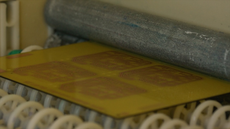
But as we delve into new areas, like flexible electronics, established wiring methods will no longer meet our needs. This will increasingly hinder forward progress and prevent large-scale adoption of wearable devices such as health monitors and medical devices.
The working principle and optical system of bubble printing (📷: M. Mukai et al.)
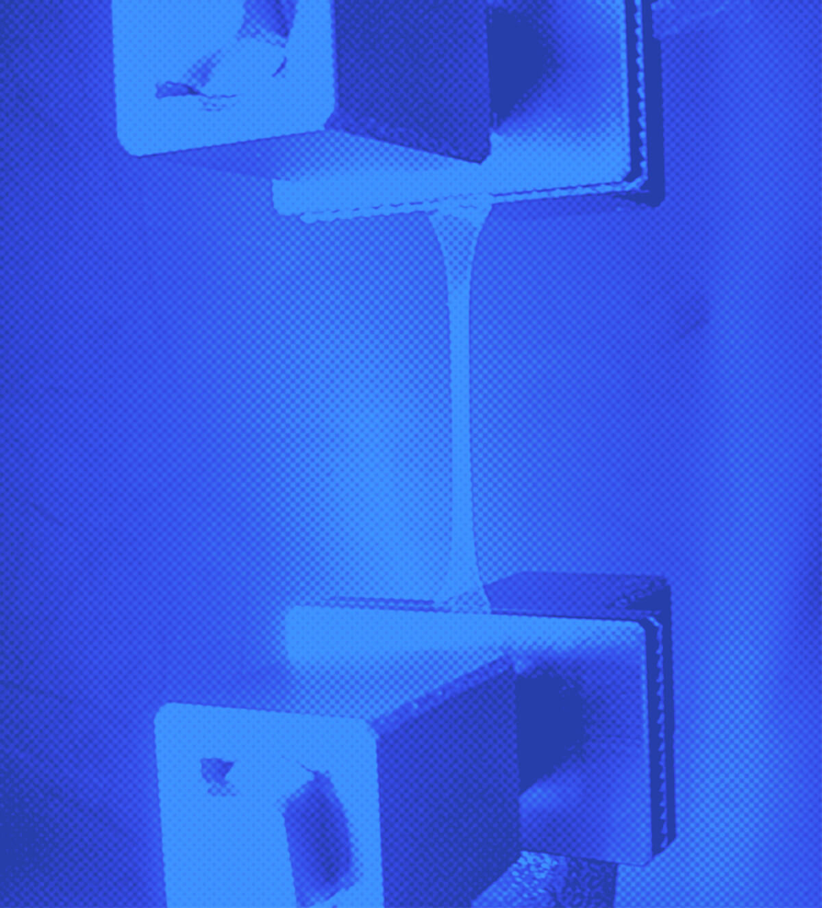
But now a team of engineers at Yokohama National University has developed a technique to fabricate wiring suitable for flexible applications that could help us to meet the needs of this next generation of devices. Their method makes use of bubble printing and liquid metal in an innovative way that can create the fine patterns necessary for modern electronic circuits. These printed wires have been demonstrated to be both highly conductive and flexible.
The process begins by using a colloidal solution of eutectic gallium-indium particles, known for their high conductivity and liquid state at room temperature. A laser is focused on this liquid, generating microbubbles that direct the particles to form specific patterns on a substrate. In this way, patterns of conductive traces can be formed with great precision.
Galvanic replacement greatly increases conductivity (📷: M. Mukai et al.)
However, because these particles have an insulating oxide film, they need further treatment to become conductive. This is achieved through a galvanic replacement process, where the oxide layer is replaced with a silver layer by immersing the patterns in a silver nitrate solution. By controlling laser intensity and scan patterns, this method can produce wiring with various line widths and shapes, allowing for precise and scalable patterning for flexible electronics.
The team’s approach simplifies the production of complex wiring patterns and enhances the wiring’s conductivity and flexibility, showing great potential for a variety of advanced applications in flexible electronics.
link


More Stories
Researchers Reveal Molecular Secrets of Flexible Electronics
Growth Outweighs Uncertainty for Flexible and Printed Electronics: OE-A Survey
SEMI FlexTech Announces 2026 FLEXI Award Winners